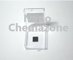
CVD Graphene
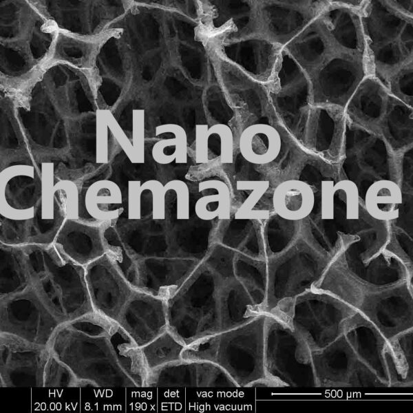
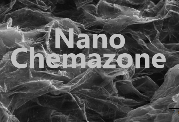
3D Freestanding Graphene Foam
| Product Name |
3D Freestanding Graphene Foam |
| Stock No. | NCZ-GSW-0023 |
| Purity | > 99.9% |
| Graphene Film | |
| FET Electron Mobility on Al2O3 | 2000 cm2/Vs |
| Hall Electron Mobility on SiO2/Si | 4000 cm2/Vs |
| Sheet Resistance | <600Ω/sq |
| Custom Order | <300Ω/sq |
| Transparency | >95% |
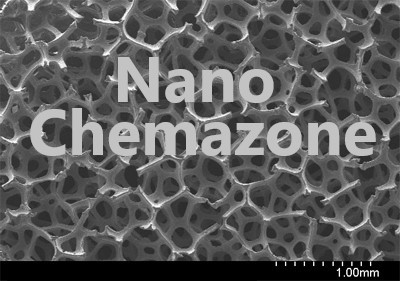
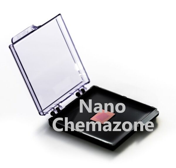
3D Graphene on Nickel/Copper Foam
CAS No.: 7782-42-5 (graphene), 7440-02-0 (nickel)
| Sheet Resistance | <600Ω/sq |
| Custom Order | <300Ω/sq |
| Transparency | >95% |
| Product Name |
3D Graphene on Nickel/Copper Foam |
| Stock No. | NCZ-GSW-0022 |
| Purity | > 99.9% |
| Graphene Film | |
| FET Electron Mobility on Al2O3 | 2000 cm2/Vs |
| Hall Electron Mobility on SiO2/Si | 4000 cm2/Vs |
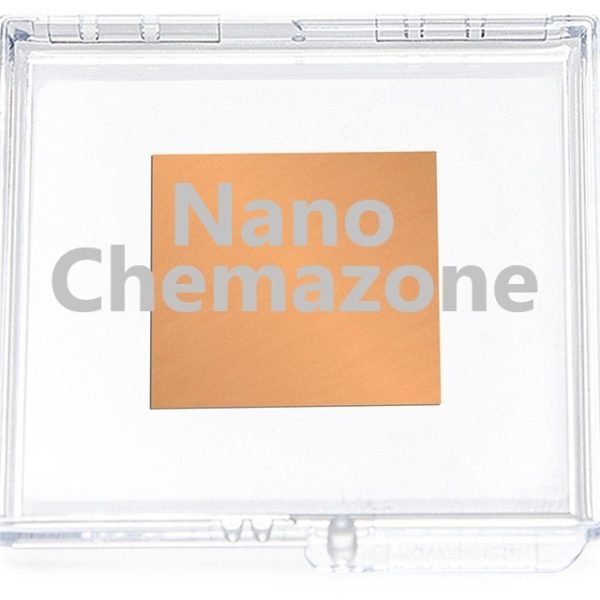
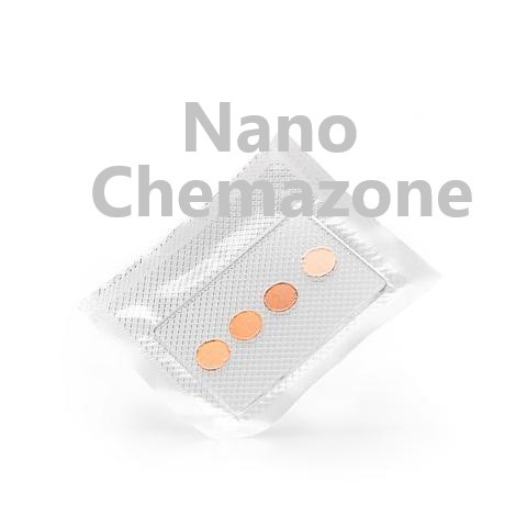
CVD Graphene on Copper Foil
CAS No.: 7782-42-5 (graphene), 7440-50-8 (copper)
PREPARATION METHOD: CVD Method
WAFER STRUCTURE: Graphene on Copper Foil (both sides), Copper Foil 45 µm
CHARACTERIZATION & ANALYSIS
Predominantly Single-layer Graphene on Copper Substrate
| Sheet Resistance | <600Ω/sq |
| Custom Order | <300Ω/sq |
| Transparency | >95% |
| Product Name |
CVD Graphene on Copper Foil |
| Stock No. | NCZ-GSW-0016 |
| Purity | > 99.9% |
| Graphene Film | |
| FET Electron Mobility on Al2O3 | 2000 cm2/Vs |
| Hall Electron Mobility on SiO2/Si | 4000 cm2/Vs |

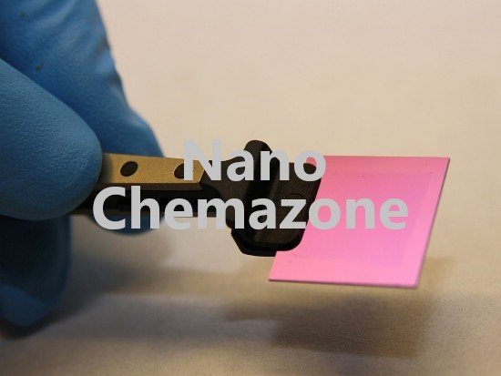
CVD Graphene on PET Substrate
| Product Name |
CVD Graphene on PET Substrate |
| Stock No. | NCZ-GSW-0019 |
| Purity | > 99.9% |
| Graphene Film | |
| FET Electron Mobility on Al2O3 | 2000 cm2/Vs |
| Hall Electron Mobility on SiO2/Si | 4000 cm2/Vs |
| Sheet Resistance | <600Ω/sq |
| Custom Order | <300Ω/sq |
| Transparency | >95% |
CVD Graphene on Quartz Substrate
| Product Name |
CVD Graphene on Quartz Substrate |
| Stock No. | NCZ-GSW-0020 |
| Purity | > 99.9% |
| Graphene Film | |
| FET Electron Mobility on Al2O3 | 2000 cm2/Vs |
| Hall Electron Mobility on SiO2/Si | 4000 cm2/Vs |
| Sheet Resistance | <600Ω/sq |
| Custom Order | <300Ω/sq |
| Transparency | >95% |
| CVD Graphene | Substrate |
| 1cm x 1cm | Diameter: 1inch, Thickness: 3mm* |
| 1inch x 1inch | 30mm x 30mm, Thickness: 1mm |
CVD Graphene on Silicon Substrate
| Product Name |
CVD Graphene On Silicon Substrate |
| Stock No. | NCZ-GSW-0017 |
| Purity | > 99.9% |
| Graphene Film | |
| FET Electron Mobility on Al2O3 | 2000 cm2/Vs |
| Hall Electron Mobility on SiO2/Si | 4000 cm2/Vs |
| Sheet Resistance | 450±40 Ω/sq (1cm x1cm) |
| Transparency | >95% |
- Copper-based graphene is prepared by CVD method.
- Graphene is transferred from copper to silicon substrate.
SILICON WAFER:
| Wafer Thickness: | 525 µm, (customization is possible) |
| Resistivity: | <0.01 ohm-cm |
| Type/Dopant: | P/N |
| Orientation: | <100> (customization is possible) |
| Front Surface: | Polished |
| Back Surface: | Etched |

CVD Graphene on SiO2 Substrate
| Product Name |
CVD Graphene on SiO2 Substrate/Wafer |
| Stock No. | NCZ-GSW-0018 |
| Purity | > 99.9% |
| Graphene Film | |
| FET Electron Mobility on Al2O3 | 2000 cm2/Vs |
| Hall Electron Mobility on SiO2/Si | 4000 cm2/Vs |
| Sheet Resistance | <600Ω/sq |
| Custom Order | <300Ω/sq |
| Transparency | >95% |
| CVD Graphene | Substrate |
| 1cm x 1cm | 1.5cm x 1.5cm, thickness: 300nm SiO2/700um Si |
| 1inch x 1inch | 3.0cm x 3.0cm, thickness: 300nm SiO2/700um Si |
| 3cm x 3cm | 3.5cm x 3.5cm, thickness: 300nm SiO2/700um Si |
| 7cm x 7cm | Diameter: 4inch, thickness: 300nm SiO2/600um Si |
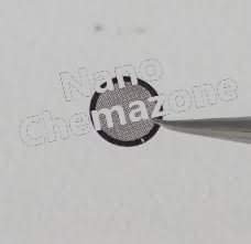
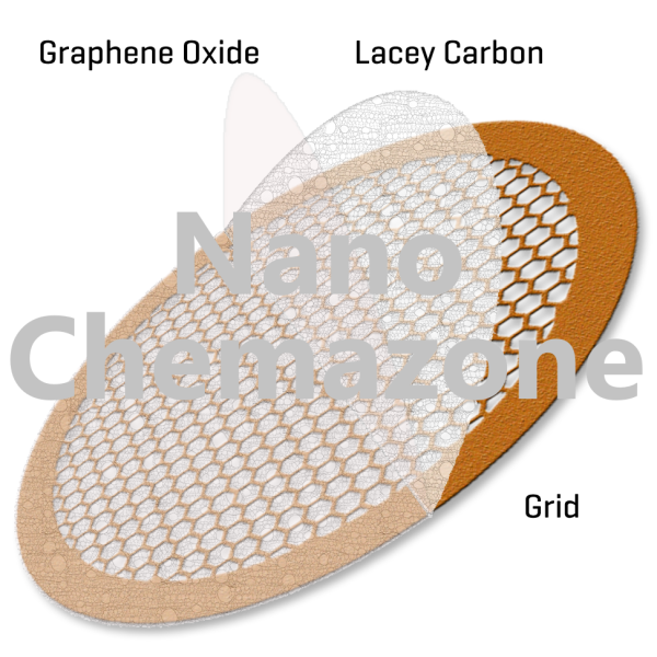
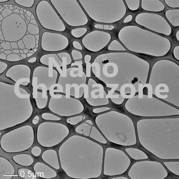
Graphene on Lacey Carbon 300 Mesh Copper TEM Grids
Graphene On Lacey Carbon 300 Mesh Copper TEM Grids
| Product Name | Graphene On Lacey Carbon 300 Mesh Copper TEM Grids |
| Stock No. | NCZ-GSW-0015 |
| Purity | > 99.9% |
| Graphene Film | |
| FET Electron Mobility on Al2O3 | 2000 cm2/Vs |
| Hall Electron Mobility on SiO2/Si | 4000 cm2/Vs |
| Sheet Resistance | 450±40 Ω/sq (1cm x1cm) |
- Four thicknesses of CVD graphene: Available in either 1, 2, 3-5 or 6-8 layers
- TEM Substrate: Lacey carbon support film on 300 mesh copper TEM grid
- Graphene coverage of the TEM grid is better than 75%
| Type | Thickness of the Graphene | Transparency | TEM Grid/AFM Substrate | Support Film |
| 1 Layer | ~0.35 nm | ~96.4% | 300 Mesh Copper Grid | N/A |
| 2 Layers | ~0.7 nm | ~92.7% | 300 Mesh Copper Grid | N/A |
| 3-5 Layers | 1.0-1.7 nm | ~85.8-90.4% | 300 Mesh Copper Grid | N/A |
| 6-8 Layers | 2.1-2.8 nm | ~78.5-83.2% | 300 Mesh Copper Grid | N/A |

Graphene on Silicon Nitride TEM Grids
Graphene on Silicon Nitride TEM Grids
| Product Name | Graphene on Silicon Nitride TEM Grids |
| Stock No. | NCZ-GSW-0012 |
| Purity | > 99.9% |
| Graphene Film | |
| FET Electron Mobility on Al2O3 | 2000 cm2/Vs |
| Hall Electron Mobility on SiO2/Si | 4000 cm2/Vs |
| Sheet Resistance | 450±40 Ω/sq (1cm x1cm) |
- Four thicknesses of CVD graphene: Available in either 1, 2, 3-5 or 6-8 layers
- TEM Substrate: 200 µm thick 3.0mm hexagonal silicon substrate with a 0.5x0.5mm aperture and 200nm thick silicon nitride membrane with approximately 6,400 2.5µm holes
- Graphene coverage of the TEM grid is > 75%
| Type | Thickness of the Graphene | Transparency | TEM Grid/AFM Substrate | Support Film |
| 1 Layer | ~ 0.35 nm | ~ 96.4% | 2.5 μm Hole Silicon Nitride | Silicon Nitride |
| 2 Layers | ~0.7 nm | ~92.7% | 2.5 μm Hole Silicon Nitride | Silicon Nitride |
| 3-5 Layers | 1.0-1.7 nm | ~85.8-90.4% | 2.5 μm Hole Silicon Nitride | Silicon Nitride |
| 6-8 Layers | 2.1-2.8 nm | ~78.5-83.2% | 2.5 μm Hole Silicon Nitride | Silicon Nitride |
Graphene on SiO2 Substrate
Graphene on Ultra-Flat Thermal SiO2 Substrate
| Product Name | Graphene on Ultra-Flat Thermal SiO2 Substrate |
| Stock No. | NCZ-GSW-0011 |
| Purity | > 99.9% |
| Graphene Film | |
| FET Electron Mobility on Al2O3 | 2000 cm2/Vs |
| Hall Electron Mobility on SiO2/Si | 4000 cm2/Vs |
| Sheet Resistance | 450±40 Ω/sq (1cm x1cm) |
- Four thicknesses of CVD graphene: Available in either 1, 2, 3-5 or 6-8 layers
- The Ultra-flat Thermal SiO2 Substrate consists of a 200 nm thermally grown SiO2 film on an ultra-flat silicon wafer with a normal thickness of 675 µm. The size is 5mm x 5mm.
- Graphene coverage of the TEM grid is 75-95 %
| Type | Thickness of the Graphene | Transparency | Support Film |
| 1 Layer | ~0.35nm | ~96.4% | Ultra-flat Silicon |
| 2 Layers | ~0.7nm | ~92.7% | Ultra-flat Silicon |
| 3-5 Layers | 1.0-1.7nm | ~85.8-90.4% | Ultra-flat Silicon |
| 6-8 Layers | 2.1-2.8nm | ~78.5-83.2% | Ultra-flat Silicon |

Graphene on Ultra-Fine 200 Mesh Copper TEM Grids
Graphene coated TEM Grids
| Product Name | Graphene On Ultra-Fine 200 Mesh Copper TEM Grids |
| Stock No. | NCZ-GSW-0014 |
| Purity | > 99.9% |
| Graphene Film | |
| FET Electron Mobility on Al2O3 | 2000 cm2/Vs |
| Hall Electron Mobility on SiO2/Si | 4000 cm2/Vs |
| Sheet Resistance | 450±40 Ω/sq (1cm x1cm) |
- Four thicknesses of CVD graphene: Available in either 1, 2, 3-5 or 6-8 layers
- TEM Substrate: Microporous Copper TEM Grids with Beryllium-Copper Support Aperture
- Graphene coverage of the TEM grid is better than 75%
| Type | Thickness of the Graphene | Transparency | TEM Grid/AFM Substrate | Support Film |
| 1 Layer | ~0.35 nm | ~96.4% | 200 Mesh Copper Grid | N/A |
| 2 Layers | ~0.7 nm | ~92.7% | 200 Mesh Copper Grid | N/A |
| 3-5 Layers | 1.0-1.7 nm | ~85.8-90.4% | 200 Mesh Copper Grid | N/A |
| 6-8 Layers | 2.1-2.8 nm | ~78.5-83.2% | 200 Mesh Copper Grid | N/A |