Other Products
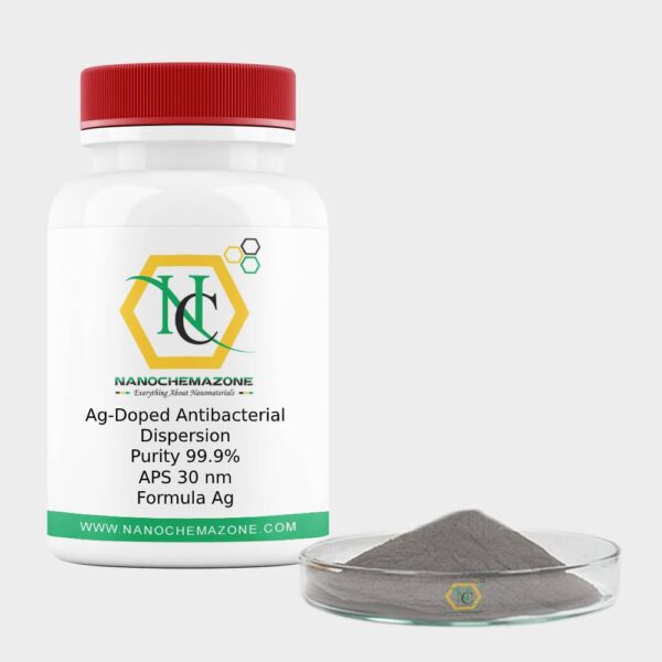
Ag-Doped Antibacterial Nanopowder Dispersion
Ag-Doped Antibacterial Nanopowder Dispersion
| Product | Ag-Doped Antibacterial Nanopowder Dispersion |
| CAS No. | 7440-22-4 |
| Appearance | Gary |
| Purity | 99.9% |
| APS | 30 nm(Can be customized) |
| Ingredient | Ag |
| Product Code | NCZ-NSC430/20 |
Ag-Doped Antibacterial Nanopowder Dispersion Description :
Ag-Doped Antibacterial Nanopowder Dispersion is nanoparticles of silver of between 1 nm and 100 nm in size. While frequently described as being 'silver' some are composed of a large percentage of silver oxide due to their large ratio of surface to bulk silver atoms.
Numerous shapes of Ag-doped Antibacterial Nanopowder Dispersion can be constructed depending on the application at hand. Commonly used silver nanoparticles are spherical, but diamond, octagonal, and thin sheets are also common.
Their extremely large surface area permits the coordination of a vast number of ligands. The properties of silver nanoparticles applicable to human treatments are under investigation in laboratory and animal studies, assessing potential efficacy, toxicity, and costs.
The most common methods for nanoparticle synthesis fall under the category of wet chemistry or the nucleation of particles within a solution.
This nucleation occurs when a silver ion complex, usually Ag-Doped Antibacterial Nanopowder Dispersion, is reduced to colloidal silver in the presence of a reducing agent. When the concentration increases enough, dissolved metallic silver ions bind together to form a stable surface.
The surface is energetically unfavorable when the cluster is small because the energy gained by decreasing the concentration of dissolved particles is not as high as the energy lost from creating a new surface.
When the cluster reaches a certain size, known as the critical radius, it becomes energetically favorable, and thus stable enough to continue to grow.
This nucleus then remains in the system and grows as more silver atoms diffuse through the solution and attach it to the surface.
When the dissolved concentration of atomic silver decreases enough, it is no longer possible for enough atoms to bind together to form a stable nucleus.
At this nucleation threshold, new nanoparticles stop being formed, and the remaining dissolved silver is absorbed by diffusion into the growing nanoparticles in the solution.
As the particles grow, other molecules in the solution diffuse and attach to the surface. This process stabilizes the surface energy of the particle and blocks new silver ions from reaching the surface.
The attachment of these capping/stabilizing agents slows and eventually stops the growth of the particle.
The most common capping ligands are trisodium citrate and polyvinylpyrrolidone (PVP), but many others are also used in varying conditions to synthesize particles with particular sizes, shapes, and surface properties.
There are many different wet synthesis methods, including the use of reducing sugars, nitrate reduction, reduction via sodium borohydride.
The silver mirror reaction, the polyol process, seed-mediated growth, and light-mediated growth. Each of these methods, or a combination of methods, will offer differing degrees of control over the size distribution as well as distributions of geometric arrangements of the nanoparticle.
Ag-Doped Antibacterial Nanopowder Dispersion Related Information
Storage Conditions: Airtight sealed, avoid light and keep dry at room temperature. Please contact us for customization and price inquiry Email: contact@nanochemazone.com Note: We supply different size ranges of Nano and micron as per the client’s requirements and also accept customization in various parameters.
Antimony Tin oxide Powder
Antimony Tin oxide Powder
Product Name: Antimony Tin oxide powder| Product | Antimony Tin oxide powder |
| Colour | White |
| Purity | ≥ 99.9% |
| Particle size | 1-10 µM (customizable) |
| Ingredient/MF | SnO2, Sb2O3 |
| Product Code | NCZ-CM-176/20 |
| CAS Number | 18282-10-5/1309-64-4 |
- ATO has excellent electrical and optical properties that are widely used as good electrical conductivity, also as an antistatic agent widely used in paint, chemical fiber, polymer film field.
- ATO has good insulation properties. Used the ATO coating to be made of automotive glass is an excellent effect of shielding and reflecting infrared radiation.
- ATO with super fine conductive properties can be used in paints, textiles, plastics, and other fields, the direct mixing of liquid and configuration system, good compatibility.
- ATO has excellent electrical and optical properties. Used as an antistatic agent is widely used in paint, chemical fiber, polymer film field.
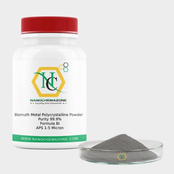
Bismuth Metal Polycrystalline Powder
Product Name: Bismuth Metal Polycrystalline Powder
| Product | polycrystalline |
| CAS No. | 7440-69-9 |
| Appearance | brown Powder |
| Purity | 99.9% |
| APS | 1 – 5 Microns (Can be customized) |
| Ingredient | Bi |
| Product Code | NCZ-NSC-275/20 |

Gallium Nitride Powder
Product Name: Gallium Nitride Powder
| Product | Gallium Nitride |
| CAS No. | 25617-97-4 |
| Appearance | Yellow Powder |
| Purity | 99.9% |
| APS | 1 – 5 Microns (Can be customized) |
| Ingredient | GaN |
| Product Code | NCZ-NSC-135/20 |
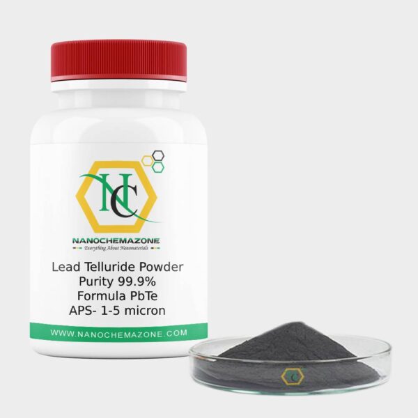
Lead Telluride Powder
Product Name: Lead Telluride Powder
| Product | Lead Telluride Powder |
| CAS No. | 1314-91-6 |
| Appearance | Grey Powder |
| Purity | 99.9% |
| APS | 1 – 5 Microns (Can be customized) |
| Ingredient | PbTe |
| Product Code | NCZ-NSC-140/20 |
Lead Telluride Description :
Lead tin telluride is a ternary alloy of lead, tin, and tellurium, generally made by alloying either tin into lead telluride or lead into tin telluride. It is a narrow bandgap semiconductor material.
The bandgap is tuned by varying the composition(x) in the material. SnTe can be alloyed with Pb (or PbTe with Sn) to tune the bandgap from (SnTe). Lead Telluride Powder important to note that unlike chalcogenides, e.g. cadmium, mercury, and zinc chalcogenides, the bandgap in Te does not change linearly between the two extremes. In contrast, as the composition (x) is increased, the bandgap decreases approach zero in the concentration regime (0.32–0.65 corresponding to temperature 4-300 K, respectively) and further increases towards the bulk bandgap of SnTe. Therefore, the lead-tin telluride alloys have narrower band gaps than their endpoint counterparts making lead tin telluride an ideal candidate for mid-infrared, 3–14 μm optoelectronic application.
Lead Telluride Powder has a positive temperature coefficient i.e. for a given composition x, the bandgap increases with temperature. Therefore, temperature stability has to be maintained while working with lead-tin telluride based laser. However, the advantage is that the operating wavelength of the laser can simply be tuned by varying the operating temperature.
The optical absorption coefficient of lead-tin telluride is typical ~750 cm−1 as compared to ~50 cm−1 for the extrinsic semiconductors such as doped silicon. The higher optical coefficient value not only ensures higher sensitivity but also reduces the spacing required between individual detector elements to prevent optical cross-talk making integrated circuit technology easily.
Lead Telluride Related Information
Storage Conditions: Airtight sealed, avoid light and keep dry at room temperature. Please email us for the customization. Email: contact@nanochemazone.com Note: We supply different size ranges of nano and micron size powder as per the client’s requirements and also accept customization in various parameters.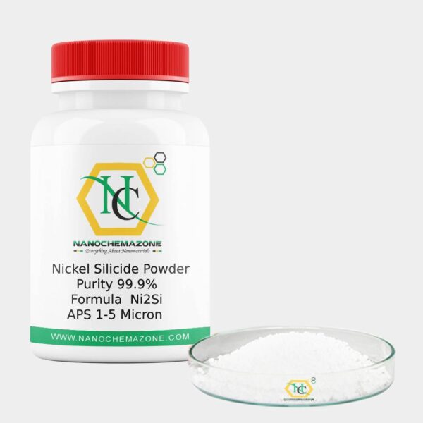
Nickel Silicide Powder
Nickel Silicide Powder
Product Name: Nickel Silicide Powder
| Product | Nickel Silicide Powder |
| CAS No | 12059-14-2 |
| Appearance | White Powder |
| Purity | 99.9% |
| APS | 1 – 5 Microns (Can be customized) |
| Ingredient | Ni2Si |
| Product Code | NCZ-NSC-133/20 |
Nickel Silicide Powder Related Information:
Nickel Silicide Powder: The reaction between SiC with chemically plated nickel on its surface has been investigated. X-ray analysis gave a good number of lattice parameters for Ni 3Si, a = 0.3522nm, and has good agreement with the index. The surface layer of Ni diffuses into the SiC and exothermically forms Ni 3Si in a defined temperature range, producing free carbon which could be deleterious to the properties.
A reaction is evident at temperatures 900°C and 1350°C with an increasing trend. The mechanism of sintering which is shown to be a reaction sintered transient-liquid phase method was determined by thermal analysis and metallographic techniques. The strength, hardness, and density properties of sintered Ni /Al (Liquid) + SiC composites are also reported.
Storage Conditions: Airtight sealed, avoid light and keep dry at room temperature. Please email us for the customization. Email: contact@nanochemazone.com Note: We supply different size ranges of nano and micron size powder as per the client’s requirements and also accept customization in various parameters.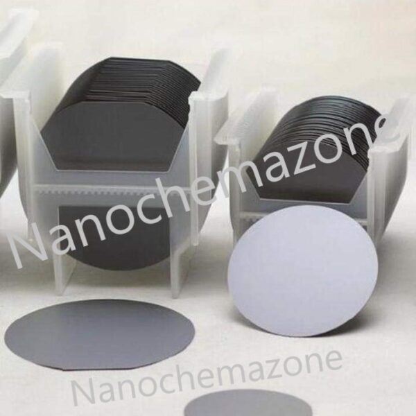
Silicon oxide wafer P-Type (2 inch)
Product Name: Silicon oxide wafer P-Type (2 inches)
| Product Name | Silicon oxide wafer P-Type (2 inches) |
| Cat. No. | NCZ-NSC318/20 |
| Diameter | 50.8+- 0.2 mm (2 inch) |
| Oxide Thickness | 300 +- 20 nm (dry) |
| Resistivity | (1-10 Ohm/sq). |
| Thickness | 300+ 15 µm |
| Orientation | <100>+- 0.5 |
Silicon oxide wafer P-Type (2 inches) Description
Provided in Single wafer caseSingle Crystal Silicon for solar energy applications includes p-type and n-type silicon. Silicon Silicon-based photovoltaic cells (PV Cells) for solar energy are fabricated from a positively charged or p-type silicon layer underneath a negatively charged or n-type silicon layer. These layers can be produced from single crystal silicon material sold under the AE Solar Energy group. Most silicon-based PV solar cells are produced from polycrystalline silicon with single-crystal systems the next most common. Silicon Metal is also available as a polycrystalline powder for casting, amorphous silicon for deposition, disc, granules, ingot, pellets, pieces, powder, rod, sputtering target, wire, and other forms and custom shapes. Ultra-high purity and high purity forms also include submicron powder and nanoscale powder. Single Crystal Silicon is generally immediately available in most volumes.
Silicon oxide wafer P-Type (2 inches) RELATED INFORMATION
Storage Conditions: Airtight sealed, avoid light, and keep dry at room temperature. Please email us for the customization. Email: contact@nanochemazone.com Note: We supply different size ranges of nano and micron size powder as per the client’s requirements and also accept customization in various parameters.
Single Crystal Silicon Wafer N-Type
Single Crystal Silicon Wafer N-Type (1 inch)
Product Name: Single Crystal Silicon Wafer N-Type (1 inch)
| Product Name | Single Crystal Silicon Wafer N-Type (1 inch) |
| Cat No. | NCZ-NSC330/20 |
| Size | 1 inch |
| Thickness | 300-380 micro-meter |
| Type | N-type |
| Dopant | Phosphorus |
| Resistivity | 1-10 ohm/cm |
| Surface | Single side polished |
| Boling Point | 2355 °C (lit.) |
| Melting Point | 1240 °C,1410 °C (lit.) |
| Density | 2.33 g/mL at 25 °C (lit.) |
| Semiconductor Properties | <100>, N-type |
| SMILES string | [Si] |
Single Crystal Silicon Wafer N-Type (1 inch). We have heated polished doped single-crystal silicon wafers in a single-mode microwave cavity to temperatures where surface to surface bonding occurred. The absorption of microwaves and heating of the wafers is attributed to the inclusion of n-type or p-type impurities into these substrates.
A cylindrical cavity TM (sub 010) standing wave mode was used to irradiate samples of various geometry at positions of high magnetic field. This process was conducted in a vacuum to exclude plasma effects.
This initial study suggests that the inclusion of impurities in single crystal silicon significantly improved its microwave absorption (loss factor) to a point where heating silicon wafers directly can be accomplished in minimal time. Bonding of these substrates, however, occurs only at points of intimate surface to surface contact. The inclusion of a thin metallic layer on the surfaces enhances the bonding process.
Please email us for the customization. Email: contact@nanochemazone.com Please contact us for customization and price inquiry Note: We supply different size ranges of Nano and micron as per the client’s requirements and also accept customization in the various parameters
Single crystal silicon wafer N-type (2 inch)
Single crystal silicon wafer N-type (2 inch)
Product Name: Single crystal silicon wafer N-type (2 inch)
| Product Name | Single crystal silicon wafer N-type (2 inch) |
| Cat No. | NCZ-NSC332/20 |
| Diameter | 2 inch |
| Doping | N type |
| Resistivity | (1-10 Ohm/sq). |
| Thickness | 290 + 10 µm |
| Orientation | 100 |
| Polished | Single side polished |
| Form | crystalline (cubic (a = 5.4037) |
| Polished | wafer (single side polished |
| does not contain | dopant |
| dia | 2 inch |
| Thickness | 0.5 mm |
| Boling Point | 2355 °C (lit.) |
| Melting Point | 1410 °C (lit.) |
| Density | 2.33 g/mL at 25 °C (lit.) |
| Semiconductor properties | <100>, N-type |
| SMILES string | [Si] |
Single crystal silicon wafer N-type (2 inch) Nanochemazone® Supplies provides both standard and customized high-quality single crystals, wafers and substrates for a wide range of applications such as LED, ferroelectric, piezoelectric, electro-optical, photonics, high power electronics, and high-frequency power devices, just to name a few. Customized crystal growth, precision machining, and coating services are available. Please contact us today to discuss your project requirements.
Please email us for the customization. Email: contact@nanochemazone.com Please contact us for customization and price inquiry Note: We supply different size ranges of Nano and micron as per the client’s requirements and also accept customization in the various parameters.
Single Crystal Silicon-Silicon dioxide Wafer
Single Crystal silicon-silicon dioxide Wafer
Product Name: Single Crystal silicon-silicon dioxide Wafer
| Product Name | Single Crystal silicon-silicon dioxide Wafer P-type (4 inches) |
| Cat No. | NCZ-NSC318/20 |
| Día | 100 mm (4 inches) |
| Orientation | <100> |
| Wafer thickness | 500 micrometer |
| Resistivity | <0.01 |
| Polished | Front Side Polished |
| Thickness | 300 nm (dry) |
| Purity | 99.9% |
| Formula | Si/SiO2 |
Single Crystal silicon-silicon dioxide Wafer P-type Description :
Provided in a single wafer caseSilicon oxide wafer SIO2 thin-film among semiconductor technology, SiO2 thin film layers are mainly used as dielectric material and more recently, they are integrated with MEMS (Micro Electro Mechanical Systems) devices. The simplest way to produce silicon oxide layers on silicon wafers is to oxidize silicon with oxygen.
Single Crystal silicon-silicon dioxide Wafer RELATED INFORMATION Storage Conditions: Airtight sealed, avoid light and keep dry at room temperature. Please email us for the customization. Email: contact@nanochemazone.com Note: We supply different size ranges of nano and micron size powder as per the client’s requirements and also accept customization in various parameters.
Titanate-Lithium Titanium Oxide Nanopowder
Product Name: Lithium Titanate-Lithium Titanium Oxide Nanopowder
Please email us for the customization.
Email: contact@nanochemazone.com
Please contact us for customization and price inquiry
Note: We supply different size ranges of Nano and micron as per the client’s requirements and also accept customization in various parameters.
Titanate-Lithium Titanium Oxide Nanopowder
| Product | Titanate-Lithium Titanium Oxide Nanopowder |
| Colour | White |
| Purity | ≥ 99.99% |
| Particle size | 1-10 µM(customizable) |
| Ingredient/MF | Li4Ti5O12 |
| Product Code | NCZ-CK-189/20 |
| CAS Number | 12031-82-2/ 12031-95-7 |